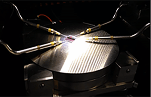
The Nano@HMU Division is working at the frontiers of nanoscience and solution advanced materials towards the industrialization of emerging printed electronics, photonics, energy harvesting and storage devices. NANO@HMU is renowned for its achievements on interfacial engineering of emerging solar cells, such as perovskite and organic, for improved performance and stability, and on their performance evaluation in outdoor conditions. The division has superior know-how on the formulation and printing of solution processable graphene and other 2D related crystals, as well as on their functionalization and doping for fine tuning of their energy levels and work-function. The research topics of Nano@HMU are the following:
Graphene and related 2D layered materials
Solution-phase processing of graphene and dichalcogenides for additive manufacturing platforms. Formulation of printable/sprayable 2D materials and multicomponent heterostructures with tailored properties through chemical functionalization and doping processes. Understanding functionalization/doping mechanisms and optimizing interfaces for improving device performance.
Organic & perovskite solar cells
Development of non-fullerene acceptors organic and perovskite solar cells. Interfacial engineering of solution processable solar cells for improved performance and stability. Study of charge transfer dynamics and fundamental understanding of mechanisms of degradation. Adaption of low temperature and cost processes, targeting to short energy and CO2 payback times.
Industrialization of emerging PVs
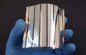
Development and engineering of transferable to industry roll-to-roll (R2R) and sheet-to-sheet (S2S) printing processes. Indoor and outdoor characterization and monitoring of PV modules and panels with IEC and ISOS protocols. Correlation of environmental data with PV performance under real and standardized conditions and side-by-side benchmark with other PV technologies.
Printed & Flexible electronics
Development of printed electronics (TFTs, foldable OLEDs, sensors), supported miniaturized circuits, portable energy devices and assembly of self-powered, flexible platforms for agriculture, smart wearables, IoT and industry 4.0 applications. Development of in-situ characterization techniques to measure material properties.
Scalable Manufacturing Processes
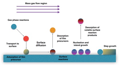
Design, simulation and implementation of a technology that is proven to be industrially competitive – that of Chemical Vapour Deposition in several variants including atmospheric pressure CVD, low-pressure CVD and plasma-enhanced CVD. Production of materials with high yield uniformity and improved efficiency in combination with a significant reduction in operational and maintenance cost.
Electrodes for Energy Storage and Smart Material Applications
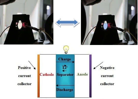
Design and control of the structural morphology and phase composition of electrode materials towards a better understanding of the material vs. property relationship. Quality assessment of nanocomposite materials through the controlled study of a) layer thickness and layer number, b) surface roughness and chemistry, c) interfacial combinations, d) defect concentration and distribution and their effect on electrode ion storage.
Materials for Photocatalysis and Fuel Cells
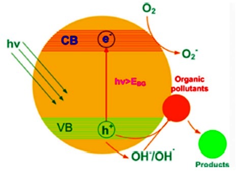
Preparation of materials as powders and thin layers via solution processing, with tailored characteristics as far as roughness, crystallinity and grain size dispersion are concerned. Photocatalytic activity studies with gas and liquid pollutants. Understanding of photocatalyst architectures in correlation with their proven efficiency. Investigation of the testing protocol necessary to study the effect of parameters such as humidity, airflow regime, light source, catalyst loadings, concentrations on the reduction of selected pollutants in a lab-scale reactor.

